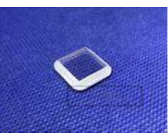
Wearable Synthetic Ruby Custom Shape Red Titanium Sapphire Laser Crystals - China
price: check with company for price
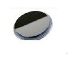
2#, 5# grade red Titanium sapphire laser crystals Ruby optical glass raw lens ingot by customized shape - - - - Parameters of materials | | Materials | Ti3+: Al2O3 | | Concentrations | (0.05~0.35)wt%Ti2O3 | | Orientation | A-Axis, C-axis within 3 | | End Configuration | flat/flat or Brewster/Brewster ends | | Absorption Coefficence | 0.5~6.0cm-1 | | Figure of Merit | 100~300 | | Coatings | Standard coating is BBAR with R < 5.0% each face at 532 nm and R < 0.5% each face, 650 nm to 850 nm.
Other coatings available.
| - - - - - - - - max size | dia120x200mml(Cz method)100kg for KY method | Mass density | 3.98 g/cm3 | Moh hardness | 9 | Young's modulus | 335 GPa | Tensile strength | 400 MPa | Melting point | 2040C | Thermal conductivity | 33 W/(mK) | Thermal expansion coefficient | 510-6K-1 | Thermal shock resistance parameter | 790 W/m | Refractive index at 633 nm | 1.76 | Temperature dependence of refractive index | 1310-6K-1 | Ti density for 0.1% at.
doping | 4.561019cm-3 | Concentrations | (0.05~0.35) wt% | End Configuration | Flat/Flat or Brewster/Brewster ends | Emission cross section at 790 nm (polarization parallel to the c axis) | 4110-20cm2 | | | - - - - Features of optics instruments Ti sapphire for christmas lights laser Large gain-bandwidth Very large emission bandwidth Excellent thermal conductivity Short excited-state lifetime (3.2 s) High saturation power Relatively high laser cross-sections High damage threshold Strong Kerr effect Wide possible pump wavelengths Applications of optics instruments Ti sapphire for christmas lights laser Femtosecond pulse lasers High repetition rate oscillators Chirped-pulse laser amplifiers Multi-pass amplifiers Regenerative amplifiers Wavelength tunable CW lasers Pulsed X-ray generation Thin disk oscillator Petawatt laser systems Specification of optics Ti sapphire lens - - - - Property | Value | Orientation Tolerence | < 3 | Thickness/Diameter Tolerance | 0.03 mm | Surface Flatness | <@632 nm | Wavefront Distortion | <@632 nm | Surface Quality | 20/10, 40/20 | Parallel | 30 | Perpendicular | 15 | Clear Aperture | >90% | Chammfer | <0.245 | Maximum dimensions | dia 120mm | - - - - Pictures size spec Grade: optical grade without bubble, size: (pictures sizes)40x40x50mml, dia100x20mmt, (dia1~100mm ok) Orientation: C(0001)0.5, surface: polished/lapped either ok color grade: (picture)block5#, ingot 2#, About our company ZMKJlocates in the city of Shanghai, Which is the best city of China, and our factory is founded in Wuxicity in 2014 - We specialize in processing a varity of materials into wafers, substrates and custiomized optical glass parts.
components widely used in electronics, optics, optoelectronics and many other fields.
We also have been working closely with many domestic and oversea universities, research institutions and companies, provide customized products and services for their R&D projects.
It's our vision tomaintaining a good relationship of cooperation with our all customers by our good reputatiaons.
FAQ: Q1 - Is your company a factory or trade company? We have a factory and we also can do export ourself.
We are the Sapphire Window manufactuer.
Q2 - Is you company only work with sapphire business? no, at present our company work with sapphire business and other semiconductor materials as like sic, LT, GaAs.
but We process sapphire components and Ruby components as the center of gravityat present.
Q3 - Could you supply sample? Yes, we can supply sapphire sample according to customer's requirement.
Q4 - Do you have any stock of sapphire window? We process sapphire window according to customer requirement.
So we have few sapphire window in stock.
Q5 - Where is your company located? Our company located in shanghai, China.
factory is in Wuxi city.
Q6 - How long will take to get the products? Generally it will take 2~4 weeks to process.
It is depend on the quantity and the size of the sapphire products.
Company Contact:
- Posted By: SHANGHAI FAMOUS TRADE CO.,LTD
- Phone: 86-512-36829962
- Address: Rm1-607,No.231,Lvdi Road, Huaqiao town, Kunshan city,jiangsu Province, Kunshan , Jiangsu , China
- Email:

- Website: https://www.galliumnitridewafer.com
Published date: March 19, 2018
- Business Description: As a result of our high quality products and outstanding customer service, we have gained a global sales network reaching If you are interested in any of our products or would like to discuss a custom order, please feel free to contact us.
Related listings
-
 Al2o3 Crystal Sapphire Cover Glass Double Side Polished Customized ShapeMetal treatment machinery - SHANGHAI FAMOUS TRADE CO.,LTD - China - March 19, 2018 - 5.00 Dollar US$
sapphire wafer, for led substrates, sapphie optical windows, Al2O3 crystal glass lens by double side polished. Sapphirecharacter 1.high temperature resistant, Sapphire Round / Rectangular Optical Window can work under 1200C continuously, and in short...
-
 Dia 50 8mm 2 Inch Gallium Arsenide Wafer For Semiconductor SubstrateMetal treatment machinery - SHANGHAI FAMOUS TRADE CO.,LTD - China - March 19, 2018 - check with company for price
2inch GaAs substrates, GaAs wafer for led, Gallium Arsenide crystal Wafers, Si/Zn Dopant GaAs wafer(A compound of the elements gallium and arsenic. It is a III-V direct bandgap semiconductor with a zinc blende crystal structure) Application: 1. Mainl...
-
 Undoped Semi Insulating Gallium Nitride Wafer Hvpe And Template TypeMetal treatment machinery - SHANGHAI FAMOUS TRADE CO.,LTD - China - March 19, 2018 - check with company for price
2inch HVPE method Gallium Nitride GaN wafer, free standing GaN substrates for LD, 10x10mm size GaN chips, HVPE GaN wafer About GaN FeatureIntroduce - - - - The growing demand for high-speed, high-temperature and high power-handling capabilities has m...
Safe Trade Tips
- Ask for business references and check them
- Use a payment method that offers better protection for all such as Letters of credit and verified professional escrow services. Avoid payments in advance such as money transfers
- Verify their business via their local Chamber of Commerce
- Search the internet using their website address, their business name, their phone and fax numbers, and their email addresses to see if you can find any feedback about them.
- Get to know more about scams and fraud to avoid: Internet Crime Complaint Center - Consumer Financial Protection Bureau
- This site is never involved in any transaction, and does not handle payments, shipping, guarantee transactions, provide escrow services, or offer "buyer protection" or "seller certification"